
Articles liés à The Source/Drain Engineering of Nanoscale Germanium-based...
Synopsis
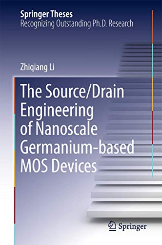
This book mainly focuses on reducing the high parasitic resistance in the source/drain of germanium nMOSFET. With adopting of the Implantation After Germanide (IAG) technique, P and Sb co-implantation technique and Multiple Implantation and Multiple Annealing (MIMA) technique, the electron Schottky barrier height of NiGe/Ge contact is modulated to 0.1eV, the thermal stability of NiGe is improved to 600? and the contact resistivity of metal/n-Ge contact is drastically reduced to 3.8×10⁻⁷O•cm2, respectively. Besides, a reduced source/drain parasitic resistance is demonstrated in the fabricated Ge nMOSFET. Readers will find useful information about the source/drain engineering technique for high-performance CMOS devices at future technology node.
Les informations fournies dans la section « Synopsis » peuvent faire référence à une autre édition de ce titre.
À propos de l'auteur
Dr. Li received his Bachelor degree of Science from Sichuan University in 2009, and Ph.D from Peking University in 2014
Prizes and awards:
2009-2014, Peking University
Leo KoGuan Scholarship, Chenming Hu Scholarship, Merit Student, Creative Talent Award.
2005-2009, Sichuan University
National Scholarship (twice), National Encouragement Scholarship, Xinyuan Scholarship (twice),
Comprehensive First-class Scholarship, Excellent Student Leader.
Publications:
1. Zhiqiang Li, Xia An, Min Li, Quanxin Yun, Meng Lin, Ming Li, Xing Zhang, and Ru Huang, “Low Electron Schottky Barrier Height of NiGe/Ge Achieved by Ion-Implantation after Germanidation Technique,” IEEE Electron Device Lett.,vol. 33, no. 12, pp. 1687–1689, Dec. 2012.
2. Zhiqiang Li, Xia An, Min Li, Quanxin Yun, Meng Lin, Ming Li, Xing Zhang, and Ru Huang, “Morphology and Electrical Performance Improvement of NiGe/Ge Contact by P and Sb Co-implantation,” IEEE Electron Device Lett., vol. 34, no. 5, pp. 596–598, May. 2013.
3. Zhiqiang Li, Xia An, Quanxin Yun, Meng Lin, Min Li, Ming Li, Xing Zhang, and Ru Huang, “Low Specific Contact Resistivity to n-Ge and Well-Behaved Ge n?/p Diode Achieved by Multiple Implantation and Multiple Annealing Technique,” IEEE Electron Device Lett., vol. 34, no. 9, pp. 1097–1099, Sep. 2013.
4. Zhiqiang Li, Xia An, Quanxin Yun, Meng Lin, Xing Zhang and Ru Huang, “Tuning Schottky Barrier Height in Metal/n-Type Germanium by Inserting an Ultrathin Yttrium Oxide Film,” ECS Solid State Lett., Vol. 1, no. 4, pp. Q33-Q34, 2012.
5. Zhiqiang Li, Xia An, Min Li, Quanxin Yun, Meng Lin, Ming Li, Xing Zhang, and Ru Huang, “Study on Schottky Barrier Modulation of NiGe/Ge by Ion-implantation after Germanidation Technique,” The 11th ICSICT, Xi’an, 2012.
À propos de la quatrième de couverture
This book mainly focuses on reducing the high parasitic resistance in the source/drain of germanium nMOSFET. With adopting of the Implantation After Germanide (IAG) technique, P and Sb co-implantation technique and Multiple Implantation and Multiple Annealing (MIMA) technique, the electron Schottky barrier height of NiGe/Ge contact is modulated to 0.1eV, the thermal stability of NiGe is improved to 600? and the contact resistivity of metal/n-Ge contact is drastically reduced to 3.8×10⁻⁷O cm2, respectively. Besides, a reduced source/drain parasitic resistance is demonstrated in the fabricated Ge nMOSFET. Readers will find useful information about the source/drain engineering technique for high-performance CMOS devices at future technology node.
Les informations fournies dans la section « A propos du livre » peuvent faire référence à une autre édition de ce titre.
Résultats de recherche pour The Source/Drain Engineering of Nanoscale Germanium-based...

Image d'archives
The Source/Drain Engineering of Nanoscale Germanium-based MOS Devices (eng)
impression à la demandeVendeur : Brook Bookstore On Demand, Napoli, NA, Italie
Évaluation du vendeur 5 sur 5 étoiles

Etat : new. Questo è un articolo print on demand. N° de réf. du vendeur 5c334e27a871d94d98a9ee6d8bb7062c
Acheter neuf
EUR 46,22
Expédition à EUR 5,50
Expédition depuis Italie vers Etats-Unis
Expédition depuis Italie vers Etats-Unis
Quantité disponible : Plus de 20 disponibles
Image fournie par le vendeur
The Source/Drain Engineering of Nanoscale Germanium-based MOS Devices
Edité par
Springer Berlin Heidelberg Jun 2016, 2016
ISBN 10 : 366249681X
ISBN 13 : 9783662496817
Neuf
Couverture rigide
Vendeur : BuchWeltWeit Ludwig Meier e.K., Bergisch Gladbach, Allemagne
Évaluation du vendeur 5 sur 5 étoiles
Buch. Etat : Neu. This item is printed on demand - it takes 3-4 days longer - Neuware -This book mainly focuses on reducing the high parasitic resistance in the source/drain of germanium nMOSFET. With adopting of the Implantation After Germanide (IAG) technique, P and Sb co-implantation technique and Multiple Implantation and Multiple Annealing (MIMA) technique, the electron Schottky barrier height of NiGe/Ge contact is modulated to 0.1eV, the thermal stability of NiGe is improved to 600 and the contact resistivity of metal/n-Ge contact is drastically reduced to 3.8×10⁻⁷ -cm2, respectively. Besides, a reduced source/drain parasitic resistance is demonstrated in the fabricated Ge nMOSFET. Readers will find useful information about the source/drain engineering technique for high-performance CMOS devices at future technology node. 80 pp. Englisch. N° de réf. du vendeur 9783662496817
Acheter neuf
EUR 53,49
Expédition à EUR 23
Expédition depuis Allemagne vers Etats-Unis
Expédition depuis Allemagne vers Etats-Unis
Quantité disponible : 2 disponible(s)
Image d'archives
The Source/Drain Engineering of Nanoscale Germanium-based MOS Devices (Springer Theses) [Hardcover] Li, Zhiqiang
Edité par
Springer, 2016
ISBN 10 : 366249681X
ISBN 13 : 9783662496817
Ancien ou d'occasion
Couverture rigide
Edition originale
Vendeur : SpringBooks, Berlin, Allemagne
Évaluation du vendeur 5 sur 5 étoiles
Hardcover. Etat : As New. 1. Auflage. Unread, like new. Immediately dispatched from Germany. N° de réf. du vendeur CEA-2406C-KUECHSTAPEL-02-0500k
Acheter D'occasion
EUR 29,95
Expédition à EUR 49,90
Expédition depuis Allemagne vers Etats-Unis
Expédition depuis Allemagne vers Etats-Unis
Quantité disponible : 1 disponible(s)
Image d'archives
The Source/Drain Engineering of Nanoscale Germanium-based MOS Devices (Springer Theses)
Vendeur : Books Puddle, Woodside, NY, Etats-Unis
Évaluation du vendeur 4 sur 5 étoiles

Etat : New. pp. 59. N° de réf. du vendeur 26375557158
Acheter neuf
EUR 81,04
Expédition à EUR 3,58
Expédition nationale : Etats-Unis
Expédition nationale : Etats-Unis
Quantité disponible : 4 disponible(s)
Image d'archives
The Source/Drain Engineering of Nanoscale Germanium-based MOS Devices (Springer Theses)
impression à la demandeVendeur : Majestic Books, Hounslow, Royaume-Uni
Évaluation du vendeur 4 sur 5 étoiles
Etat : New. Print on Demand pp. 59. N° de réf. du vendeur 370488313
Acheter neuf
EUR 82,59
Expédition à EUR 7,77
Expédition depuis Royaume-Uni vers Etats-Unis
Expédition depuis Royaume-Uni vers Etats-Unis
Quantité disponible : 4 disponible(s)
Image d'archives
The Source/Drain Engineering of Nanoscale Germanium-based MOS Devices (Springer Theses)
impression à la demandeVendeur : Biblios, Frankfurt am main, HESSE, Allemagne
Évaluation du vendeur 4 sur 5 étoiles
Etat : New. PRINT ON DEMAND pp. 59. N° de réf. du vendeur 18375557164
Acheter neuf
EUR 82,87
Expédition à EUR 9,95
Expédition depuis Allemagne vers Etats-Unis
Expédition depuis Allemagne vers Etats-Unis
Quantité disponible : 4 disponible(s)
Image fournie par le vendeur
The Source/Drain Engineering of Nanoscale Germanium-based MOS Devices
Edité par
Springer Berlin Heidelberg, 2016
ISBN 10 : 366249681X
ISBN 13 : 9783662496817
Neuf
Couverture rigide
Vendeur : moluna, Greven, Allemagne
Évaluation du vendeur 5 sur 5 étoiles
Gebunden. Etat : New. N° de réf. du vendeur 117108279
Acheter neuf
EUR 48,37
Expédition à EUR 48,99
Expédition depuis Allemagne vers Etats-Unis
Expédition depuis Allemagne vers Etats-Unis
Quantité disponible : Plus de 20 disponibles
Image fournie par le vendeur
The Source/Drain Engineering of Nanoscale Germanium-based MOS Devices
Vendeur : AHA-BUCH GmbH, Einbeck, Allemagne
Évaluation du vendeur 5 sur 5 étoiles
Buch. Etat : Neu. Druck auf Anfrage Neuware - Printed after ordering - This book mainly focuses on reducing the high parasitic resistance in the source/drain of germanium nMOSFET. With adopting of the Implantation After Germanide (IAG) technique, P and Sb co-implantation technique and Multiple Implantation and Multiple Annealing (MIMA) technique, the electron Schottky barrier height of NiGe/Ge contact is modulated to 0.1eV, the thermal stability of NiGe is improved to 600 and the contact resistivity of metal/n-Ge contact is drastically reduced to 3.8×10⁻⁷ -cm2, respectively. Besides, a reduced source/drain parasitic resistance is demonstrated in the fabricated Ge nMOSFET. Readers will find useful information about the source/drain engineering technique for high-performance CMOS devices at future technology node. N° de réf. du vendeur 9783662496817
Acheter neuf
EUR 66,40
Expédition à EUR 35
Expédition depuis Allemagne vers Etats-Unis
Expédition depuis Allemagne vers Etats-Unis
Quantité disponible : 1 disponible(s)
Image fournie par le vendeur
The Source/Drain Engineering of Nanoscale Germanium-based MOS Devices
Edité par
Springer, Springer Jun 2016, 2016
ISBN 10 : 366249681X
ISBN 13 : 9783662496817
Neuf
Couverture rigide
Vendeur : buchversandmimpf2000, Emtmannsberg, BAYE, Allemagne
Évaluation du vendeur 5 sur 5 étoiles
Buch. Etat : Neu. This item is printed on demand - Print on Demand Titel. Neuware -This book mainly focuses on reducing the high parasitic resistance in the source/drain of germanium nMOSFET. With adopting of the Implantation After Germanide (IAG) technique, P and Sb co-implantation technique and Multiple Implantation and Multiple Annealing (MIMA) technique, the electron Schottky barrier height of NiGe/Ge contact is modulated to 0.1eV, the thermal stability of NiGe is improved to 600¿ and the contact resistivity of metal/n-Ge contact is drastically reduced to 3.8×10¿7¿¿cm2, respectively. Besides, a reduced source/drain parasitic resistance is demonstrated in the fabricated Ge nMOSFET. Readers will find useful information about the source/drain engineering technique for high-performance CMOS devices at future technology node.Springer-Verlag KG, Sachsenplatz 4-6, 1201 Wien 80 pp. Englisch. N° de réf. du vendeur 9783662496817
Acheter neuf
EUR 53,49
Expédition à EUR 60
Expédition depuis Allemagne vers Etats-Unis
Expédition depuis Allemagne vers Etats-Unis
Quantité disponible : 1 disponible(s)